- 您现在的位置:买卖IC网 > Sheet目录1992 > DAC8413EP (Analog Devices Inc)IC DAC 12BIT QUAD V-OUT 28-DIP
Quad, 12-Bit DAC
Voltage Output with Readback
Data Sheet
FEATURES
+5 V to ±15 V operation
Unipolar or bipolar operation
True voltage output
Double-buffered inputs
Reset to minimum (DAC8413) or center scale (DAC8412)
Fast bus access time
Readback
APPLICATIONS
Automatic test equipment
Digitally controlled calibration
Servo controls
Process control equipment
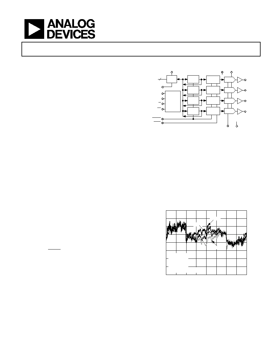
FUNCTIONAL BLOCK DIAGRAM
DGND
A0
A1
CS
RESET
LDAC
12
I/O
PORT
CONTROL
LOGIC
DATA
I/O
R/W
INPUT
REG A
INPUT
REG B
INPUT
REG C
INPUT
REG D
OUTPUT
REG A
OUTPUT
REG B
OUTPUT
REG C
OUTPUT
REG D
DAC A
DAC B
DAC C
DAC D
VLOGIC
VDD VREFH
VREFL VSS
VOUTA
VOUTB
VOUTC
VOUTD
00274-
001
Figure 1.
GENERAL DESCRIPTION
The DAC8412/DAC8413 are quad, 12-bit voltage output
DACs with readback capability. Built using a complementary
BiCMOS process, these monolithic DACs offer the user very
high package density.
Output voltage swing is set by the two reference inputs VREFH
and VREFL. By setting the VREFL input to 0 V and VREFH to a
positive voltage, the DAC provides a unipolar positive output
range. A similar configuration with VREFH at 0 V and VREFL at a
negative voltage provides a unipolar negative output range.
Bipolar outputs are configured by connecting both VREFH and
VREFL to nonzero voltages. This method of setting output voltage
range has advantages over other bipolar offsetting methods
because it is not dependent on internal and external resistors
with different temperature coefficients.
Digital controls allow the user to load or read back data from any
DAC, load any DAC, and transfer data to all DACs at one time.
An active low RESET loads all DAC output registers to midscale
for the DAC8412 and zero scale for the DAC8413.
The DAC8412/DAC8413 are available in 28-lead plastic DIP,
28-lead ceramic DIP, 28-lead PLCC, and 28-lead LCC packages.
They can be operated from a wide variety of supply and reference
voltages with supplies ranging from single +5 V to ±15 V, and
references from +2.5 V to ±10 V. Power dissipation is less than
330 mW with ±15 V supplies and only 60 mW with a +5 V supply.
For MIL-STD-883 applications, contact your local Analog
Devices, Inc. sales office for the DAC8412/DAC8413/883 data
sheet, which specifies operation over the 55°C to +125°C
temperature range. All 883 parts are also available on Standard
Military Drawings 5962-91 76401MXA through 76404M3A.
DIGITAL INPUT CODE (Decimal)
0.500
0.125
512
L
INE
ARI
T
Y
E
RRO
R
(
L
S
B)
0.375
–0.125
–0.250
–0.375
–0.500
0.250
0
+125°C
+25°C
–55°C
VDD = +15V
VSS = –15V
VREFH = +10V
VREFL = –10V
TA = –55°C, +25°C, +125°C
1024
1536
2046
2548
2560
3072
4096
0
00274-
002
Figure 2. INL vs. Code Over Temperature
Rev. G
Information furnished by Analog Devices is believed to be accurate and reliable. However, no
responsibilityisassumedbyAnalogDevicesforitsuse,norforanyinfringementsofpatentsorother
rightsofthirdpartiesthatmayresultfromitsuse.Specificationssubjecttochangewithoutnotice.No
license is granted by implication or otherwise under any patent or patent rights of Analog Devices.
Trademarksandregisteredtrademarksarethepropertyoftheirrespectiveowners.
One Technology Way, P.O. Box 9106, Norwood, MA 02062-9106, U.S.A.
Tel: 781.329.4700
2000–2013 Analog Devices, Inc. All rights reserved.
发布紧急采购,3分钟左右您将得到回复。
相关PDF资料
DAC8420FQ
IC DAC 12BIT QUAD SRL LP 16-CDIP
DAC8426EPZ
IC DAC 8BIT QUAD 10VREF 20PDIP
DAC8531IDRBTG4
IC D/A CONV LP 16-BIT 8-SON
DAC8562FP
IC DAC 12BIT PARALLEL 5V 20-DIP
DS1004Z-5+T
IC DELAY LINE 5TAP 25NS 8-SOIC
DS1005-125+
IC DELAY LINE 5TAP 125NS 14-DIP
DS1007S-2+T&R
IC DELAY LINE 4NS 16-SOIC
DS1010S-50+T&R
IC DELAY LINE 10TAP 16-SOIC
相关代理商/技术参数
DAC8413EPZ
功能描述:IC DAC 12BIT QUAD V-OUT 28DIP RoHS:是 类别:集成电路 (IC) >> 数据采集 - 数模转换器 系列:- 产品培训模块:Lead (SnPb) Finish for COTS
Obsolescence Mitigation Program 标准包装:1,000 系列:- 设置时间:1µs 位数:8 数据接口:串行 转换器数目:8 电压电源:双 ± 功率耗散(最大):941mW 工作温度:0°C ~ 70°C 安装类型:表面贴装 封装/外壳:24-SOIC(0.295",7.50mm 宽) 供应商设备封装:24-SOIC W 包装:带卷 (TR) 输出数目和类型:8 电压,单极 采样率(每秒):*
DAC8413FP
功能描述:IC DAC 12BIT QUAD V-OUT 28-DIP RoHS:否 类别:集成电路 (IC) >> 数据采集 - 数模转换器 系列:- 产品培训模块:Lead (SnPb) Finish for COTS
Obsolescence Mitigation Program 标准包装:1,000 系列:- 设置时间:1µs 位数:8 数据接口:串行 转换器数目:8 电压电源:双 ± 功率耗散(最大):941mW 工作温度:0°C ~ 70°C 安装类型:表面贴装 封装/外壳:24-SOIC(0.295",7.50mm 宽) 供应商设备封装:24-SOIC W 包装:带卷 (TR) 输出数目和类型:8 电压,单极 采样率(每秒):*
DAC8413FPC
功能描述:IC DAC 12BIT QUAD READBK 28-PLCC RoHS:否 类别:集成电路 (IC) >> 数据采集 - 数模转换器 系列:- 产品培训模块:Lead (SnPb) Finish for COTS
Obsolescence Mitigation Program 标准包装:1,000 系列:- 设置时间:1µs 位数:8 数据接口:串行 转换器数目:8 电压电源:双 ± 功率耗散(最大):941mW 工作温度:0°C ~ 70°C 安装类型:表面贴装 封装/外壳:24-SOIC(0.295",7.50mm 宽) 供应商设备封装:24-SOIC W 包装:带卷 (TR) 输出数目和类型:8 电压,单极 采样率(每秒):*
DAC8413FPC-REEL
功能描述:IC DAC 12BIT QUAD V-OUT 28-PLCC RoHS:否 类别:集成电路 (IC) >> 数据采集 - 数模转换器 系列:- 产品培训模块:Data Converter Fundamentals
DAC Architectures 标准包装:750 系列:- 设置时间:7µs 位数:16 数据接口:并联 转换器数目:1 电压电源:双 ± 功率耗散(最大):100mW 工作温度:0°C ~ 70°C 安装类型:表面贴装 封装/外壳:28-LCC(J 形引线) 供应商设备封装:28-PLCC(11.51x11.51) 包装:带卷 (TR) 输出数目和类型:1 电压,单极;1 电压,双极 采样率(每秒):143k
DAC8413FPCZ
功能描述:IC DAC 12BIT QUAD READBK 28-PLCC RoHS:是 类别:集成电路 (IC) >> 数据采集 - 数模转换器 系列:- 产品培训模块:Lead (SnPb) Finish for COTS
Obsolescence Mitigation Program 标准包装:1,000 系列:- 设置时间:1µs 位数:8 数据接口:串行 转换器数目:8 电压电源:双 ± 功率耗散(最大):941mW 工作温度:0°C ~ 70°C 安装类型:表面贴装 封装/外壳:24-SOIC(0.295",7.50mm 宽) 供应商设备封装:24-SOIC W 包装:带卷 (TR) 输出数目和类型:8 电压,单极 采样率(每秒):*
DAC8413FPCZ-REEL
功能描述:IC DAC 12BIT QUAD V-OUT 28PLCC RoHS:是 类别:集成电路 (IC) >> 数据采集 - 数模转换器 系列:- 产品培训模块:Data Converter Fundamentals
DAC Architectures 标准包装:750 系列:- 设置时间:7µs 位数:16 数据接口:并联 转换器数目:1 电压电源:双 ± 功率耗散(最大):100mW 工作温度:0°C ~ 70°C 安装类型:表面贴装 封装/外壳:28-LCC(J 形引线) 供应商设备封装:28-PLCC(11.51x11.51) 包装:带卷 (TR) 输出数目和类型:1 电压,单极;1 电压,双极 采样率(每秒):143k
DAC8413FPZ
功能描述:IC DAC 12BIT QUAD V-OUT 28DIP RoHS:是 类别:集成电路 (IC) >> 数据采集 - 数模转换器 系列:- 标准包装:1 系列:- 设置时间:4.5µs 位数:12 数据接口:串行,SPI? 转换器数目:1 电压电源:单电源 功率耗散(最大):- 工作温度:-40°C ~ 125°C 安装类型:表面贴装 封装/外壳:8-SOIC(0.154",3.90mm 宽) 供应商设备封装:8-SOICN 包装:剪切带 (CT) 输出数目和类型:1 电压,单极;1 电压,双极 采样率(每秒):* 其它名称:MCP4921T-E/SNCTMCP4921T-E/SNRCTMCP4921T-E/SNRCT-ND
dac8413ft
制造商:Rochester Electronics LLC 功能描述:- Bulk 制造商:Analog Devices 功能描述: